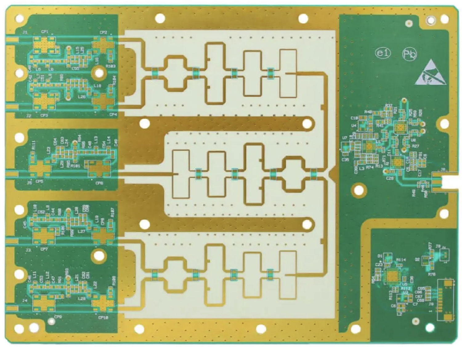

RF Microwave and digital logic boards often look different from standard circuit boards.
This is because they are used for processing or transmitting signals in the radio or microwave portion of the electromagnetic spectrum. Features often found on RF boards include edge plating, cavities, and antenna circuits.

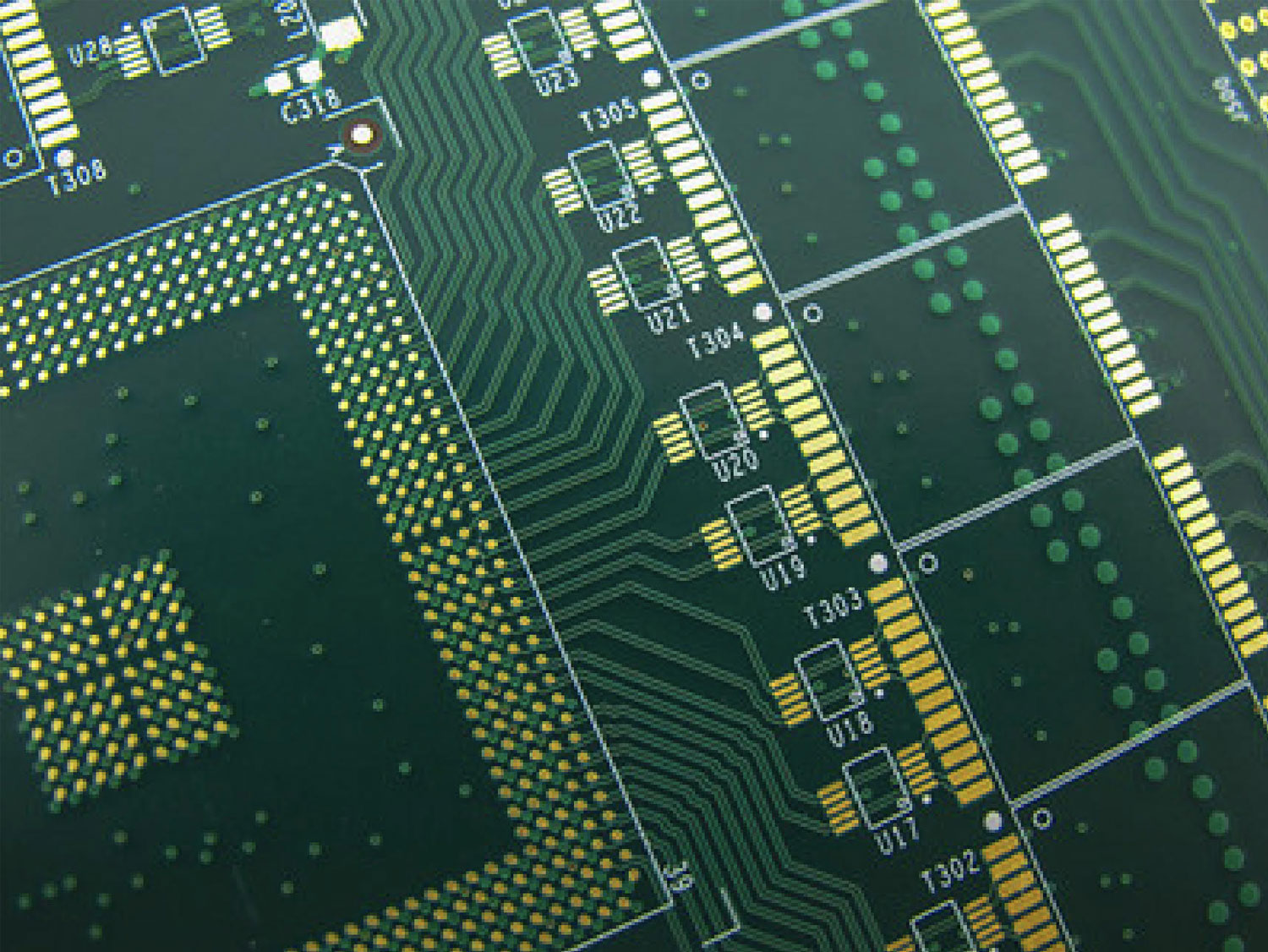
HDI stands for High-Density Interconnect and is characterized by very small copper holes and dense traces.
These are increasingly required for copper pads that interface with high-I/O components such as BGA’s, FPGA’s and LGA’s.

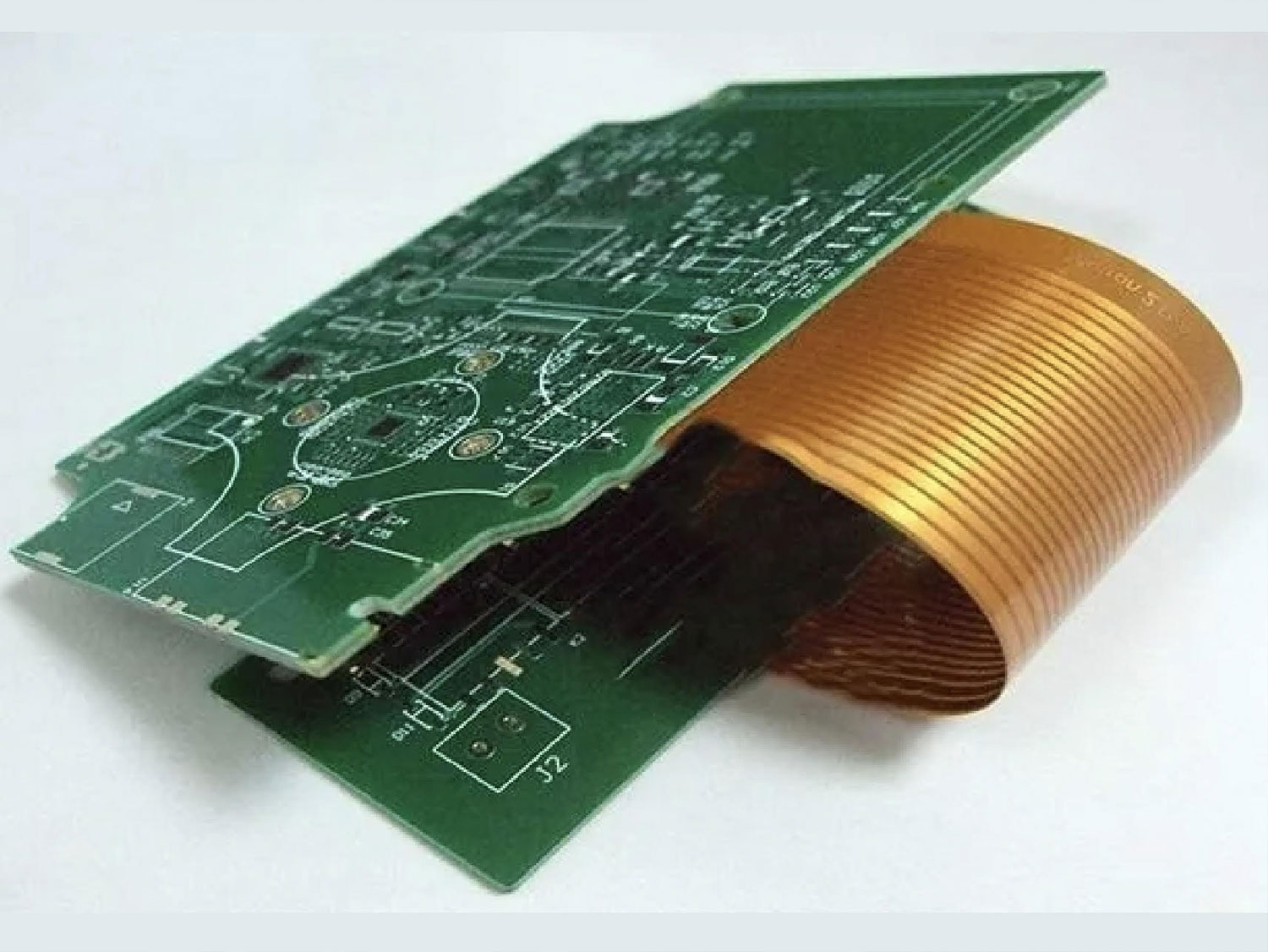
Rigid-flex PCB technology offers many benefits.First, it allows the designer to consider three-dimensional designs that wrap around mechanical housings or fit into tight spaces.
Rigid FR4 areas are combined with flexible polyimide areas to form one integrated assembly.

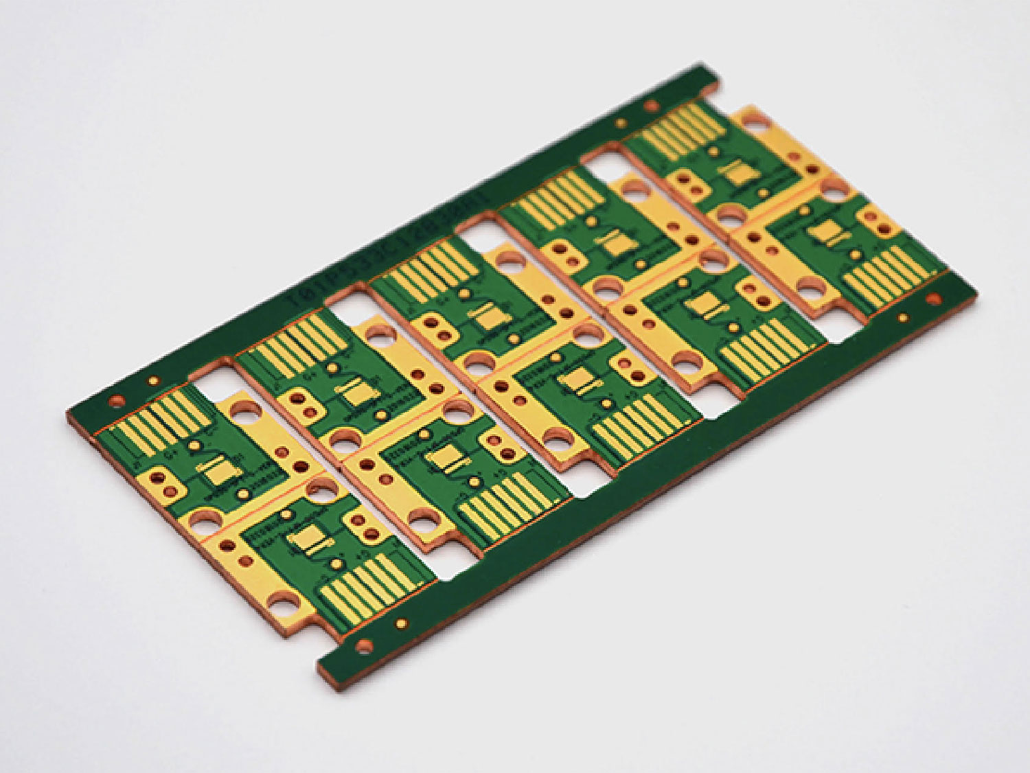
Copper in circuit boards carries the electrical current and signals.
The thickness of copper layers in PCBs is typically H oz and 1 oz.
Copper thickness is expressed in weight with 1 oz equal to .0014” or 35 µm nominal thickness. For high current and high amperage applications like power supplies, thicker copper is required. PCBs with >2 oz finished copper are considered heavy copper.